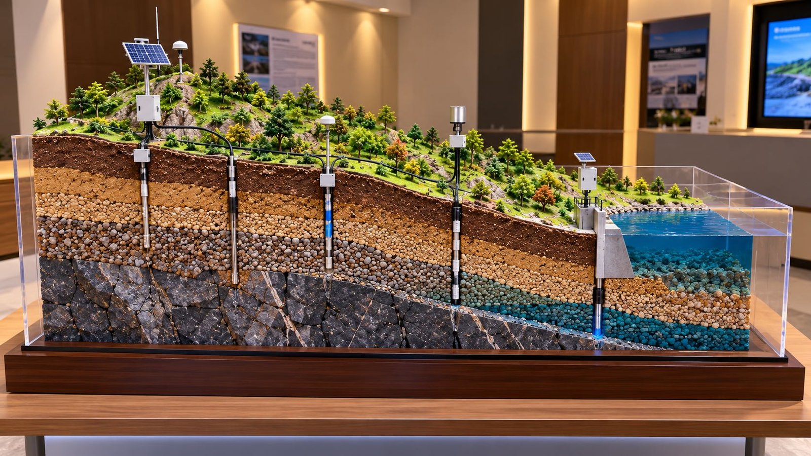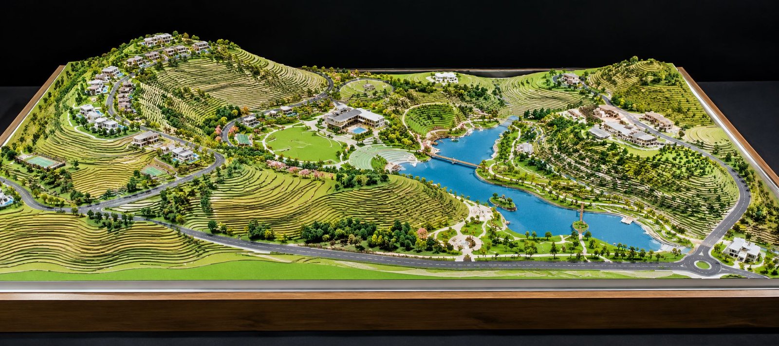
Semiconductor Manufacturing Plant Model Making in Delhi NCR
The semiconductor industry plays an important role in modern technology. Today, smartphones, computers, electric vehicles, medical equipment and industrial machines all use semiconductor components. Therefore, companies need well-planned factories to produce, assemble and test these important electronic parts.
A Semiconductor Manufacturing Plant Model provides a clear, three-dimensional view of a semiconductor factory. Instead of looking only at technical drawings, clients can see the main buildings, cleanrooms, production areas, utility facilities and internal roads in one physical model. As a result, they can understand the complete factory layout more easily.
PAL Design Models provides custom industrial, architectural and engineering scale models for different types of projects. In particular, a semiconductor plant model can help companies present a proposed factory, explain a manufacturing layout or display an industrial project in a professional way.
Delhi NCR offers useful business opportunities for industrial model making because the region includes electronics companies, engineering firms, manufacturing units, technology businesses and industrial development projects. For example, Noida, Greater Noida, Gurugram, Manesar, Ghaziabad and Faridabad are relevant locations for reaching potential clients.
Moreover, the Yamuna Expressway region is worth targeting for electronics and semiconductor-related development projects. By creating a detailed physical model, project teams can explain their designs more clearly and present important parts of the facility in one place.
What Is a Semiconductor Manufacturing Plant Model?
A semiconductor manufacturing plant model is a physical miniature version of a factory that produces or processes semiconductor devices. Depending on the project, it can show a complete manufacturing campus or a single production facility.
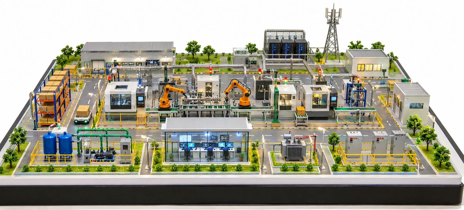
Unlike a normal building model, a semiconductor factory model includes industrial buildings and supporting systems. For instance, it may show cleanroom buildings, wafer processing areas, assembly and packaging facilities, gas storage, water treatment systems and utility buildings.
In addition, the model can include roads, security gates, parking areas, loading zones, landscaping and other site features. These details help viewers understand how different parts of the factory fit together.
The model maker develops the layout according to the client’s drawings, site plans, building designs and project requirements. Therefore, the final model can match the planned facility instead of showing a standard factory layout.
Why Is a Semiconductor Factory Scale Model Important?
Semiconductor manufacturing facilities contain many specialised buildings and support systems. Therefore, a collection of technical drawings may not give every viewer a clear picture of the complete site.
A physical semiconductor factory scale model brings the main parts of the facility together. As a result, viewers can understand the building arrangement, production areas and supporting infrastructure more easily.
Clear Three-Dimensional Presentation
A physical model shows the factory from a three-dimensional perspective. Viewers can see the building sizes, heights, roads and open areas without studying several separate drawings.
Moreover, the model can use different colours to identify important sections. For example, the main production building, utility area and water treatment facility can have separate visual details.
Better Project Communication
Project developers often need to explain their plans to clients, engineers, consultants and management teams. In these situations, a detailed semiconductor plant model provides a useful visual aid.
Furthermore, the model helps people understand how the main production buildings connect with supporting facilities. Consequently, project discussions can focus on the overall layout rather than relying only on written explanations.
Support for Factory Planning
A scale model can help project teams review the positions of major buildings, access roads and service areas. It also gives the team a shared view of the proposed facility.
However, the model does not replace engineering drawings, safety checks or technical calculations. Instead, it supports design discussions and makes the overall project easier to explain.
Professional Display for Industrial Projects
Companies may place a semiconductor manufacturing model in a reception area, meeting room, visitor centre or exhibition space.
In addition, a clean baseboard, balanced lighting and detailed miniature buildings can improve the display. As a result, the model can present the facility in a professional and organised way.
Main Components of a Semiconductor Manufacturing Plant Model
A detailed semiconductor plant model should show the main parts of the facility according to the available project drawings. The following components can be included when they match the client’s requirements.
Cleanroom and Fabrication Building
The fabrication building, also known as a semiconductor fab, is one of the most important parts of the facility.
The model can show the building’s outer walls, entrances, roof equipment, service areas and overall shape. Moreover, the designer can add selected interior details when the project requires a cutaway or sectional view.
Cleanroom facilities need a clear place in the overall layout. Therefore, their size and position should remain easy to identify.
Wafer Processing Area
The wafer processing area represents the part of the facility where manufacturers create semiconductor devices on suitable materials.
Depending on the project, the model can show this area as a separate building or as part of the main fabrication facility. In addition, miniature equipment, labels and building divisions can help identify the processing section.
These details make the model more informative without filling the baseboard with unnecessary objects.
Assembly and Packaging Facility
The assembly and packaging area supports the preparation of semiconductor devices for further testing and use in electronic products.
A semiconductor factory model can include a separate building for this activity. Furthermore, the model may show loading areas, service roads and connections to other production buildings.
As a result, viewers can understand how the assembly and packaging facility fits into the wider manufacturing campus.
Bulk Gas Storage Area
Some semiconductor manufacturing processes require special gases. Therefore, certain facilities include dedicated gas storage and supply areas.
The model can show miniature storage vessels, cylinder banks, equipment enclosures and related service structures. However, the model maker should follow the actual project layout instead of guessing technical details or safety distances.
Chemical Storage Area
Some manufacturing processes also require chemical storage and handling facilities. Where the project includes these areas, the model can show separate buildings, storage zones and suitable containment structures.
In addition, clear labels can help viewers identify these facilities. This makes the overall model easier to understand during a presentation.
Industrial Utility Buildings
Utility buildings support the operation of a semiconductor factory. Depending on the design, these facilities may include electrical equipment, cooling systems, compressed air systems and other plant services.
The model can show utility buildings, rooftop equipment, mechanical platforms and service areas. Moreover, these details give the factory a realistic industrial appearance.
Water Treatment Plant
Water treatment and water management can be important parts of semiconductor manufacturing. Depending on the production process, a facility may need water purification, storage, recycling and wastewater treatment systems.
Therefore, a detailed model may include treatment buildings, storage tanks, treatment units and related structures. The final arrangement should match the approved drawings and the client’s requirements.
Roads, Security and Landscaping
Internal roads connect the buildings and support movement across the factory campus. For this reason, roads and access points deserve careful attention.
The model may include boundary walls, security gates, pedestrian crossings, loading areas, parking spaces, miniature vehicles and streetlights. In addition, small trees and landscaped sections can improve the appearance of the campus.
A rectangular baseboard brings these elements together in a neat layout. Similarly, a wide and low-height design can show more of the factory in a website feature image.
Semiconductor Manufacturing Model Making Process
A professional model requires careful planning before fabrication begins. Therefore, the model maker should first understand the project and then select the scale, materials and level of detail.
Understanding the Project Requirements
First, the client identifies the type of facility that the model should show. It may be a semiconductor fabrication plant, an assembly and testing facility or a wider electronics manufacturing campus.
Next, the model maker reviews the available drawings, site plans, building elevations and reference images. These documents help establish the positions and sizes of the main buildings.
Furthermore, the team should understand how the client plans to use the model. For example, an exhibition model may need strong visual appeal, while an engineering presentation may require clearer details of utility areas.
Selecting the Right Scale
The correct scale depends on the size of the facility and the available display space. It also depends on the level of detail that the client wants.
For a large manufacturing campus, a smaller scale may allow all the buildings to fit on one baseboard. On the other hand, a model of a single production building may use a larger scale to show more details.
The model maker should maintain consistent proportions throughout the design. As a result, buildings, roads, storage tanks and other features will look balanced.
Developing the Three-Dimensional Layout
After reviewing the drawings, the team develops the three-dimensional layout. This stage covers building shapes, heights, roof details, access roads and supporting facilities.
Computer-aided design files can help the team work with accurate dimensions when the client supplies them. Moreover, three-dimensional references can clarify complex shapes and repeated structures.
Fabrication and Material Selection
The model maker selects materials according to the size, design and required finish.
For example, suitable sheet materials can form the buildings, while acrylic can provide transparent features. Laser cutting can produce clean and precise shapes. Similarly, 3D printing can help create specialised miniature equipment.
The main goal is to achieve accurate proportions, clean edges and a professional finish.
Painting and Adding Details
Careful painting helps distinguish the different parts of the factory. For instance, the designer can use separate colours for production buildings, utility areas and roads.
Furthermore, miniature road markings, trees, fences, streetlights and equipment details can make the model more realistic. However, the designer should avoid adding too many small objects that hide the main layout.
Lighting and Final Checking
Optional LED lighting can highlight selected buildings, entrances and roads. In addition, a well-finished baseboard can make the model look clean and organised.
Finally, the model maker checks the building positions, proportions, labels, surface finish and lighting against the agreed project brief. This review helps ensure that the finished model presents the design clearly.
Materials Used for Semiconductor Plant Scale Models
Industrial scale models use different materials to create buildings, equipment, roads and other features.
For example, PVC foam board and other suitable sheet materials can form lightweight building structures. Acrylic can create transparent elements and selected display features. Meanwhile, laser-cut parts help produce precise shapes, and 3D printing supports the production of complex miniature components.
The model maker may also use suitable materials for baseboards, roads, landscape features, storage tanks and mechanical platforms.
Moreover, the choice of material depends on the required size, appearance and level of detail. A good model should balance visual quality with clear presentation.
For semiconductor facilities, the main aim is to show the important buildings and support systems without making the layout look crowded. Therefore, the model maker should focus on the details that help viewers understand the project.
Types of Semiconductor and Electronics Models
Different projects need different types of physical models. Therefore, clients can select a model that matches their facility and presentation goals.
Semiconductor Fabrication Plant Model
This model focuses on the main fab building, cleanroom facilities, support areas and campus layout. It suits presentations that explain a proposed or existing semiconductor fabrication facility.
Semiconductor Assembly and Testing Plant Model
This model highlights assembly, packaging, testing and related support facilities. In addition, it may show loading zones, internal roads and utility buildings.
It works well for projects where assembly, packaging or testing forms the main manufacturing activity.
Electronics Manufacturing Campus Model
An electronics manufacturing campus model can show production buildings, warehouses, offices, utilities, parking and internal roads.
Cleanroom Manufacturing Facility Model
A cleanroom facility model focuses on controlled manufacturing buildings and their supporting systems.
The same general approach can also serve other specialised manufacturing sectors. However, the model should follow the actual facility design and available technical references.
Semiconductor Equipment Model
Some clients need a model of a particular machine, equipment system or manufacturing process rather than a complete factory.
In this case, a smaller engineering model may be more suitable. Moreover, the designer can include selected cutaway sections when the client provides the required drawings.
Semiconductor Manufacturing Plant Model Making in Delhi NCR
Delhi NCR offers useful business opportunities for industrial model makers because the region includes manufacturing companies, engineering firms, electronics businesses and industrial development projects.
Therefore, companies providing semiconductor plant models and factory scale models can target several locations across the region. However, each location has a different business profile, so the content should match the actual market.
Noida, Uttar Pradesh
Noida is a useful target area for electronics, technology, engineering and manufacturing-related businesses.
Companies in these sectors may need physical models for facility presentations, industrial exhibitions and project planning. In addition, engineering consultants and design firms may require models to explain factory layouts to their clients.
Relevant search topics include semiconductor manufacturing plant model maker in Noida, industrial model making company in Noida, electronics manufacturing plant model Noida and semiconductor factory scale model Noida.
Greater Noida, Uttar Pradesh
Greater Noida has an established industrial and electronics manufacturing presence. Therefore, it is a relevant area for targeting companies involved in manufacturing, engineering and industrial development.
Potential search topics include semiconductor plant model making in Greater Noida, electronics factory scale model Greater Noida, industrial scale model maker Greater Noida and manufacturing campus model making Greater Noida.
Moreover, companies developing production facilities may need models to present the layout of buildings, roads and support systems.
Yamuna Expressway and YEIDA Region
The Yamuna Expressway region is relevant to electronics and semiconductor-related development in Uttar Pradesh.
For this market, useful search topics include semiconductor plant model maker near Jewar, electronics manufacturing model Yamuna Expressway, industrial model making company YEIDA and semiconductor factory model near Noida International Airport.
However, the content should describe actual project opportunities carefully. Not every industrial site in this region is a semiconductor manufacturing facility.
Ghaziabad, Uttar Pradesh
Ghaziabad has a broad industrial and engineering business base. As a result, it is worth considering for industrial scale model making and factory presentation services.
Relevant search topics include industrial model making company in Ghaziabad, semiconductor factory model Ghaziabad, electronics plant scale model Ghaziabad and factory layout model making Ghaziabad.
In addition, equipment suppliers and engineering companies may need physical models to explain their machinery, facilities and projects.
Gurugram and Manesar, Haryana
Gurugram and Manesar are relevant to automotive, engineering, electronics and advanced manufacturing businesses.
Potential search topics include semiconductor manufacturing model in Gurugram, industrial model making company in Gurgaon, electronics manufacturing plant model Manesar and engineering scale model maker Gurugram.
Furthermore, companies working with industrial automation and manufacturing systems may need models for technical presentations and corporate displays.
Faridabad, Haryana
Faridabad is another useful area for targeting industrial and engineering companies.
Relevant search topics include industrial scale model making company Faridabad, semiconductor plant model Faridabad, factory model making services Faridabad and electronics manufacturing model Faridabad.
These searches may reach companies that need physical models of manufacturing facilities, machinery layouts and industrial equipment.
Delhi
Delhi provides access to corporate offices, industrial consultants, architecture firms, project management teams and exhibition designers.
Some of these businesses may commission models for facilities located elsewhere in NCR or in other parts of India.
Useful search topics include semiconductor plant model making company in Delhi, industrial model maker in Delhi, semiconductor factory scale model Delhi and industrial project model making Delhi NCR.
Other Industrial Locations Near Delhi NCR
Bawana, Narela, Okhla, Sahibabad, Tronica City, Kundli and Sonipat can also be considered when planning industrial model-making services.
However, these areas serve different industries. Some may offer better opportunities for general manufacturing, engineering, fabrication or warehousing projects than for semiconductor fabrication.
Therefore, it makes sense to focus first on Noida, Greater Noida, Gurugram, Manesar, Ghaziabad, Faridabad and the Yamuna Expressway region. Later, businesses can expand their targeting according to actual enquiries and website performance.
Who Needs a Semiconductor Manufacturing Plant Model?
Several types of organisations may need semiconductor plant models or related industrial scale models.
Semiconductor and Electronics Companies
Manufacturers may use physical models to present new facilities, explain factory layouts and display their manufacturing campuses. Moreover, a detailed model can help visitors understand the main parts of the site.
Architects and Industrial Designers
Architects and industrial designers can use models to explain building arrangements, service areas and site infrastructure. In addition, a physical model helps clients view the project from different angles.
EPC Contractors and Engineering Consultants
Engineering, procurement and construction teams may use industrial models to present the overall layout of a proposed facility.
As a result, clients can see how major buildings and support systems fit together before discussing individual technical details.
Industrial Park Developers
Industrial park developers may need models showing manufacturing plots, internal roads, utility areas and shared facilities.
Furthermore, a campus model can help them present the development to potential tenants, investors and project partners.
Project Management Teams
Project managers may use a physical model during planning discussions and stakeholder presentations. However, the model should support the approved project information rather than replace detailed engineering documents.
Exhibition and Display Companies
Exhibition designers may include industrial scale models in trade shows, product displays and corporate presentations.
Similarly, educational institutions may use simplified models to explain semiconductor manufacturing and related industrial systems.
How to Plan a High-Quality Semiconductor Plant Model
A clear project brief helps the model maker prepare a suitable design.
First, identify the type of facility and explain the purpose of the model. Next, provide the site plan, building layouts, elevations and reference images.
Then, decide on the physical dimensions and preferred scale. A wide, low-height layout may suit a website feature image or boardroom display. On the other hand, a model that focuses on a single building may need a different shape and level of detail.
After that, select the most important features. These may include cleanroom buildings, wafer processing areas, utility facilities, gas storage, water treatment, roads, landscaping and lighting.
In addition, confirm whether the model needs labels, a protective enclosure or removable sections. These details should match the intended display environment.
Finally, review the finished model against the supplied references. This process helps maintain accurate proportions and avoids unsupported assumptions about the facility.
SEO Strategy for Semiconductor Plant Model Making
A useful SEO strategy helps potential clients find relevant industrial model-making services through search engines.
First, create clear and helpful content about semiconductor plant models, electronics manufacturing models and cleanroom facility models. In addition, connect this content to relevant service pages on the website.
Location-based content can also help reach businesses across Delhi NCR. For example, separate pages for Noida, Greater Noida and Gurugram may be useful when each page provides original information about the local market and the service.
However, simply changing city names in identical articles does not offer much value to readers. Therefore, each location page should explain the relevant services and customer needs in a natural way.
Use descriptive image names and accurate alt text. For example, the feature image could use the file name semiconductor-manufacturing-plant-model-delhi-ncr.webp.
Furthermore, add relevant internal links to industrial model making, engineering model making, architectural model making and 3D printing pages where those services are available.
The page should also have a clear heading structure, a mobile-friendly layout and a readable URL. After publishing, check the page through Google Search Console to review its indexing status.
Frequently Asked Questions
What is a semiconductor manufacturing plant model?
A semiconductor manufacturing plant model is a physical scale version of a semiconductor factory. It can show cleanroom buildings, wafer processing areas, utility facilities, storage systems, roads and other parts of the site.
Can a semiconductor factory model be customised?
Yes. The design can follow the client’s drawings, site plans, required dimensions and preferred level of detail. In addition, the model can include selected lighting and labels when required.
Which Delhi NCR locations are useful for industrial model making?
Noida, Greater Noida, Gurugram, Manesar, Ghaziabad, Faridabad and the Yamuna Expressway region are useful areas to consider for industrial and electronics-related model-making services.
Can the model include cleanrooms and utility buildings?
Yes. The model can show cleanroom buildings, process support areas, utility facilities, gas storage and water treatment systems when the project drawings support those details.
Is a semiconductor plant model useful for presentations?
Yes. A physical model helps viewers understand the factory layout and the relationship between major buildings. Therefore, it can support project meetings, corporate displays and industrial exhibitions.
What information is required to make a semiconductor plant model?
Useful information includes site plans, architectural drawings, building elevations, reference photographs, preferred dimensions, model scale and the intended use of the finished model.
Can LED lighting be added to the model?
Yes. Optional LED lighting can highlight selected buildings, roads and display features. However, the lighting should remain balanced so that viewers can see the miniature details clearly.
Conclusion
A detailed Semiconductor Manufacturing Plant Model provides a clear physical view of a complex manufacturing facility. It brings cleanroom buildings, wafer processing areas, assembly and packaging facilities, utility systems, storage areas and site infrastructure into one presentation.
For companies looking for semiconductor manufacturing plant model making in Delhi NCR, a customised industrial scale model can support project presentations, engineering discussions, corporate displays and industrial exhibitions.
Noida, Greater Noida, Gurugram, Manesar, Ghaziabad, Faridabad and the Yamuna Expressway region offer useful markets for reaching businesses involved in electronics, engineering and industrial development.
Moreover, a well-planned model can help project teams explain their designs more clearly. By using suitable materials, accurate proportions and carefully selected details, model makers can create a professional display that matches the client’s project requirements.
Finally, useful website content, clear service information and relevant location pages can help PAL Design Models reach potential customers searching for industrial and semiconductor-related model-making services across Delhi NCR.